Archive
Dennard scaling a necessary condition for Moore’s law
Dennard scaling was a necessary, but not sufficient, condition for Moore’s law to play out over many decades. Transistors generate heat, and continually adding more transistors to a device will eventually cause it to melt, because the generated heat cannot be removed fast enough. However, if the fabrication of transistors on the surface of a monolithic silicon semiconductor follows the Dennard scaling rules, then more, smaller transistors can be added without any increase in heat generated per unit area. These scaling rules were first given in the 1974 paper Design of Ion-Implanted MOSFET’S with Very Small Physical Dimensions by Dennard, Gaensslen, Hwa-Nien, Rideout, Bassous, and LeBlanc.
The plot below shows a vertical slice through a Metal–Oxide–Semiconductor Field-Effect Transistor (the kind of transistor used to build microprocessors), with the fabrication parameters applicable to Dennard scaling labelled. A transistor has three connections (only one is show), to the Source, the Drain, and the Gate. The Source and Drain are doped with an element from Group V to produce a surplus of electrons, while the substrate is doped with an element from Group III to create holes that accept electrons. A voltage applied to the Gate creates an electric field that modifies the shape of the depletion region (area above blue dashed line), enabling the flow of electrons between the Source and Drain to be switched on or off.
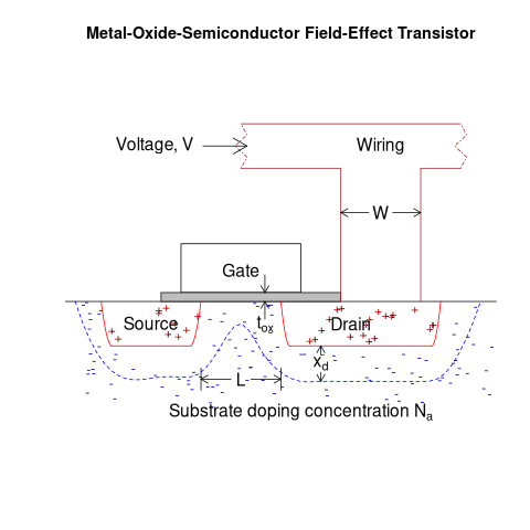
The parameters are: operating voltage,  , width of the connecting wires,
  , length of the channel between the Source and Drain,
  , thickness of the dielectric material (e.g., silicon oxynitride) under the Gate (shown in grey),
  , doping concentration,
  , and length of the depletion region,
  .
.
The power,  , consumed by any electronic device is
  , where
  is the current through it and the voltage across it. In an ideal transistor, in the off state
  and no power is consumed, and in the on state is at its maximum, but
  and no power is consumed. Power is only consumed during the transition between the two states, when both and are non-zero. In real transistors, there is some amount of leakage in the off/on states and a small amount of power is consumed.
Increasing the frequency,  , at which a transistor is operated increases the number of state transitions, which increases the power consumed. The power consumed per unit time by a transistor is
  . If there are
  transistors per unit area, the power consumed within that area is:
  .
.
The current, , can be written in terms of the factors that control it, as:  .
.
If the values of , , , and are all reduced by a factor of  (often around 30%, giving
  ), then
  is reduced by a factor of
  ,
, ^2=2") .
.
^2}}/{{L/alpha}*{t_{ox}/alpha}}}{V/alpha}={{N*f}/alpha^2}{{W*V^3}/{L*t_{ox}}}")
The area occupied by a transistor,  , decreases by , making it possible to increase the number of transistors within the same unit area to:
  . The transistors consume less power, but there are more of them, and power per unit area after the size reduction is the same as before reduction,
  .
.
Reducing the channel length, , has a detrimental impact on device performance. However, this can be overcome by increasing the density of the doping in the substrate, , by .
The maximum frequency at which a transistor can be operated is limited by its capacitance. The Gate capacitance is the major factor, and this decreases in proportion to the device dimensions, i.e., . A decrease in capacitance enables the operating frequency, , to increase. Capacitance was not included in the previous formula for power consumption. An alternative derivation finds that  , where
  is the capacitance, i.e., power consumption is unchanged when a frequency increase is matched by a corresponding decrease in capacitance.
The first working transistor was created in 1947 and the first MOSFET in 1959. The plot below, with data from various sources, shows the energy consumed by a transistor, fabricated in various years, switching between states, the red line is the fitted regression equation  , the green line is the fitted equation
  , and the grey line shows the Landauer limit for the energy consumption of a computation at room temperature (code and data; also see The End of Moore’s Law: A New Beginning for Information Technology by Theis and Wong):
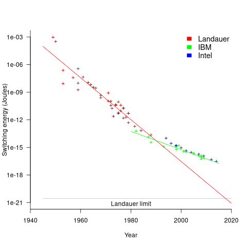
Scaling cannot go on forever. The two limits reached were voltage (difficulty reducing below 1V) and the thickness of the Gate dielectric layer (significant leakage current when less than 7 atoms thick).
The slow-down in the reduction of switching energy, in the plot above, is due to a slow-down in voltage reduction, i.e., reduction of less than .
In 2007, cpu clock frequency stopped increasing and Dennard scaling halted. In this year, the Gate and its dielectric was completely redesigned to use a high-k dielectric such as Hafnium oxide, which allowed transistor size to continue decreasing. However, since around 2014 the rate of decrease has slowed and process node numbers have become marketing values without any connection to the size of fabricated structures. Is 2014 the year that Moore’s law died? Some people think the year was 2010, while Intel still trumpet the law named after one of their founders.
Moore’s law was a socially constructed project
Moore’s law was a socially constructed project that depended on the coordinated actions of many independent companies and groups of individuals to last for as long it did.
All products evolve, but what was it about Moore’s law that enabled microelectronics to evolve so much faster and for longer than most other products?
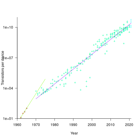
Moore’s observation, made in 1965 based on four data points, was that the number of components contained in a fabricated silicon device doubles every year. The paper didn’t make this claim in words, but a line fitted to four yearly data points (starting in 1962) suggested this behavior continuing into the mid-1970s. The introduction of IBM’s Personal Computer, in 1981 containing Intel’s 8088 processor, led to interested parties coming together to create a hugely profitable ecosystem that depended on the continuance of Moore’s law.
The plot below shows Moore’s four points (red) and fitted regression model (green line). In practice, since 1970, fitting a regression model (purple line) to the number of transistors in various microprocessors (blue/green, data from Wikipedia), finds that the number of transistors doubled every two years (code+data):
In the early days, designing a device was mostly a manual operation; that is, the circuit design and logic design down to the transistor level were hand-drawn. This meant that creating a device containing twice as many transistors required twice as many engineers. At some point the doubling process either becomes uneconomic or it takes forever to get anything done because of the coordination effort.
The problem of needing an exponentially-growing number of engineers was solved by creating electronic design automation tools (EDA), starting in the 1980s, with successive generations of tools handling ever higher levels of abstraction, and human designers focusing on the upper levels.
The use of EDA provides a benefit to manufacturers (who can design differentiated products) and to customers (e.g., products containing more functionality).
If EDA had not solved the problem of exponential growth in engineers, Moore’s law would have maxed-out in the early 1980s, with around 150K transistors per device. However, this would not have stopped the ongoing shrinking of transistors; two economic factors independently incentivize the creation of ever smaller transistors.
When wafer fabrication technology improvements make it possible to double the number of transistors on a silicon wafer, then around twice as many devices can be produced (assuming unchanged number of transistors per device, and other technical details). The wafer fabrication cost is greater (second row in table below), but a lot less than twice as much, so the manufacturing cost per device is much lower (third row in table).
The doubling of transistors primarily provides a manufacturer benefit.
The following table gives estimates for various chip foundry economic factors, in dollars (taken from the report: AI Chips: What They Are and Why They Matter). Node, expressed in nanometers, used to directly correspond to the length of a particular feature created during the fabrication process; these days it does not correspond to the size of any specific feature and is essentially just a name applied to a particular generation of chips.
Node (nm) 90 65 40 28 20 16/12 10 7 5 Foundry sale price per wafer 1,650 1,937 2,274 2,891 3,677 3,984 5,992 9,346 16,988 Foundry sale price per chip 2,433 1,428 713 453 399 331 274 233 238 Mass production year 2004 2006 2009 2011 2014 2015 2017 2018 2020 Quarter Q4 Q4 Q1 Q4 Q3 Q3 Q2 Q3 Q1 Capital investment per wafer 4,649 5,456 6,404 8,144 10,356 11,220 13,169 14,267 16,746 processed per year Capital consumed per wafer 411 483 567 721 917 993 1,494 2,330 4,235 processed in 2020 Other costs and markup 1,293 1,454 1,707 2,171 2,760 2,990 4,498 7,016 12,753 per wafer |
The second economic factor incentivizing the creation of smaller transistors is Dennard scaling, a rarely heard technical term named after the first author of a 1974 paper showing that transistor power consumption scaled with area (for very small transistors). Halving the area occupied by a transistor, halves the power consumed, at the same frequency.
The maximum clock-frequency of a microprocessor is limited by the amount of heat it can dissipate; the heat produced is proportional to the power consumed, which is approximately proportional to the clock-frequency. Instead of a device having smaller transistors consume less power, they could consume the same power at double the frequency.
Dennard scaling primarily provides a customer benefit.
Figuring out how to further shrink the size of transistors requires an investment in research, followed by designing/(building or purchasing) new equipment. Why would a company, who had invested in researching and building their current manufacturing capability, be willing to invest in making it obsolete?
The fear of losing market share is a commercial imperative experienced by all leading companies. In the microprocessor market, the first company to halve the size of a transistor would be able to produce twice as many microprocessors (at a lower cost) running twice as fast as the existing products. They could (and did) charge more for the latest, faster product, even though it cost them less than the previous version to manufacture.
Building cheaper, faster products is a means to an end; that end is receiving a decent return on the investment made. How large is the market for new microprocessors and how large an investment is required to build the next generation of products?
Rock’s law says that the cost of a chip fabrication plant doubles every four years (the per wafer price in the table above is increasing at a slower rate). Gambling hundreds of millions of dollars, later billions of dollars, on a next generation fabrication plant has always been a high risk/high reward investment.
The sales of microprocessors are dependent on the sale of computers that contain them, and people buy computers to enable them to use software. Microprocessor manufacturers thus have to both convince computer manufacturers to use their chip (without breaking antitrust laws) and convince software companies to create products that run on a particular processor.
The introduction of the IBM PC kick-started the personal computer market, with Wintel (the partnership between Microsoft and Intel) dominating software developer and end-user mindshare of the PC compatible market (in no small part due to the billions these two companies spent on advertising).
An effective technique for increasing the volume of microprocessors sold is to shorten the usable lifetime of the computer potential customers currently own. Customers buy computers to run software, and when new versions of software can only effectively be used in a computer containing more memory or on a new microprocessor which supports functionality not supported by earlier processors, then a new computer is needed. By obsoleting older products soon after newer products become available, companies are able to evolve an existing customer base to one where the new product is looked upon as the norm. Customers are force marched into the future.
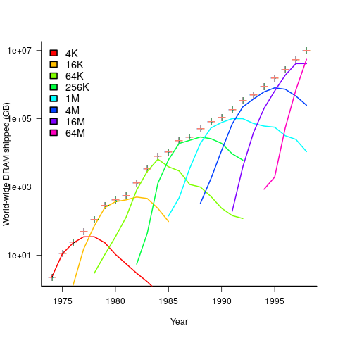
The plot below shows sales volume, in gigabytes, of various sized DRAM chips over time. The simple story of exponential growth in sales volume (plus signs) hides the more complicated story of the rise and fall of succeeding generations of memory chips (code+data):
The Red Queens had a simple task, keep buying the latest products. The activities of the companies supplying the specialist equipment needed to build a chip fabrication plant has to be coordinated, a role filled by the International Technology Roadmap for Semiconductors (ITRS). The annual ITRS reports contain detailed specifications of the expected performance of the subsystems involved in the fabrication process.
Moore’s law is now dead, in that transistor doubling now takes longer than two years. Would transistor doubling time have taken longer than two years, or slowed down earlier, if:
- the ecosystem had not been dominated by two symbiotic companies, or did network effects make it inevitable that there would be two symbiotic companies,
- the Internet had happened at a different time,
- if software applications had quickly reached a good enough state,
- if cloud computing had gone mainstream much earlier.
Recent Comments