Dennard scaling a necessary condition for Moore’s law
Dennard scaling was a necessary, but not sufficient, condition for Moore’s law to play out over many decades. Transistors generate heat, and continually adding more transistors to a device will eventually cause it to melt, because the generated heat cannot be removed fast enough. However, if the fabrication of transistors on the surface of a monolithic silicon semiconductor follows the Dennard scaling rules, then more, smaller transistors can be added without any increase in heat generated per unit area. These scaling rules were first given in the 1974 paper Design of Ion-Implanted MOSFET’S with Very Small Physical Dimensions by Dennard, Gaensslen, Hwa-Nien, Rideout, Bassous, and LeBlanc.
The plot below shows a vertical slice through a Metal–Oxide–Semiconductor Field-Effect Transistor (the kind of transistor used to build microprocessors), with the fabrication parameters applicable to Dennard scaling labelled. A transistor has three connections (only one is show), to the Source, the Drain, and the Gate. The Source and Drain are doped with an element from Group V to produce a surplus of electrons, while the substrate is doped with an element from Group III to create holes that accept electrons. A voltage applied to the Gate creates an electric field that modifies the shape of the depletion region (area above blue dashed line), enabling the flow of electrons between the Source and Drain to be switched on or off.
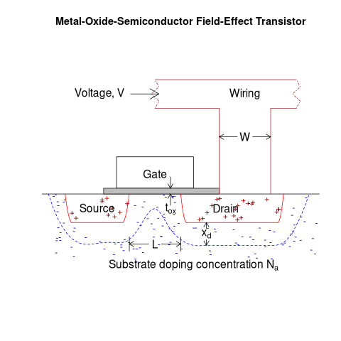
The parameters are: operating voltage,  , width of the connecting wires,
  , length of the channel between the Source and Drain,
  , thickness of the dielectric material (e.g., silicon oxynitride) under the Gate (shown in grey),
  , doping concentration,
  , and length of the depletion region,
  .
.
The power,  , consumed by any electronic device is
  , where
  is the current through it and the voltage across it. In an ideal transistor, in the off state
  and no power is consumed, and in the on state is at its maximum, but
  and no power is consumed. Power is only consumed during the transition between the two states, when both and are non-zero. In real transistors, there is some amount of leakage in the off/on states and a small amount of power is consumed.
Increasing the frequency,  , at which a transistor is operated increases the number of state transitions, which increases the power consumed. The power consumed per unit time by a transistor is
  . If there are
  transistors per unit area, the power consumed within that area is:
  .
.
The current, , can be written in terms of the factors that control it, as:  .
.
If the values of , , , and are all reduced by a factor of  (often around 30%, giving
  ), then
  is reduced by a factor of
  ,
, ^2=2") .
.
^2}}/{{L/alpha}*{t_{ox}/alpha}}}{V/alpha}={{N*f}/alpha^2}{{W*V^3}/{L*t_{ox}}}")
The area occupied by a transistor,  , decreases by , making it possible to increase the number of transistors within the same unit area to:
  . The transistors consume less power, but there are more of them, and power per unit area after the size reduction is the same as before reduction,
  .
.
Reducing the channel length, , has a detrimental impact on device performance. However, this can be overcome by increasing the density of the doping in the substrate, , by .
The maximum frequency at which a transistor can be operated is limited by its capacitance. The Gate capacitance is the major factor, and this decreases in proportion to the device dimensions, i.e., . A decrease in capacitance enables the operating frequency, , to increase. Capacitance was not included in the previous formula for power consumption. An alternative derivation finds that  , where
  is the capacitance, i.e., power consumption is unchanged when a frequency increase is matched by a corresponding decrease in capacitance.
The first working transistor was created in 1947 and the first MOSFET in 1959. The plot below, with data from various sources, shows the energy consumed by a transistor, fabricated in various years, switching between states, the red line is the fitted regression equation  , the green line is the fitted equation
  , and the grey line shows the Landauer limit for the energy consumption of a computation at room temperature (code and data; also see The End of Moore’s Law: A New Beginning for Information Technology by Theis and Wong):
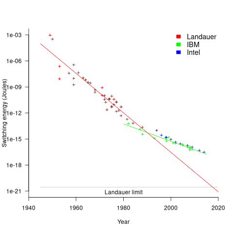
Scaling cannot go on forever. The two limits reached were voltage (difficulty reducing below 1V) and the thickness of the Gate dielectric layer (significant leakage current when less than 7 atoms thick).
The slow-down in the reduction of switching energy, in the plot above, is due to a slow-down in voltage reduction, i.e., reduction of less than .
In 2007, cpu clock frequency stopped increasing and Dennard scaling halted. In this year, the Gate and its dielectric was completely redesigned to use a high-k dielectric such as Hafnium oxide, which allowed transistor size to continue decreasing. However, since around 2014 the rate of decrease has slowed and process node numbers have become marketing values without any connection to the size of fabricated structures. Is 2014 the year that Moore’s law died? Some people think the year was 2010, while Intel still trumpet the law named after one of their founders.
You ask: “Is 2014 the year that Moore’s law died?”
Well, Herb Sutter noticed there was a problem in 2005, so that’s when I think Moore’s Law died.
See: http://gotw.ca/publications/concurrency-ddj.htm
At the time I though “This is great: we can now get back to work on writing good software.”
Whatever, we’re now in a brave new world in which it’s not the speed of the individual processor that’s important, but power dissipation per instruction. I think Apple noticed this first, but Intel seems to be jumping on the bandwagon, so I’m (perhaps overly) enthused about (the high end of) Intel’s next gen (now due out in early 2027), which will have zillions of “efficiency processors”.
Of course, that excessive enthusiasm is also due to better software, in that in the early 2000s, not much effort was put into parallelizing applications to use lots of threads. Which effort was encouraged by parallelizable apps now making up so much of current benchmark suites.
@David in Tokyo
Herb Sutter’s article discusses the switch from faster single processors (due to Dennard scaling) to multiple processors (Moore’s law continuing for a few more years). Around 2007 is when cpu heat sinks started getting larger and larger, to remove the increasing amount of heat generated by the increasing number of transistors.